Low EMI 4-layer PCB Design

Unfortunately due to NDAs I can not share any other pictures besides the partial design shown above.
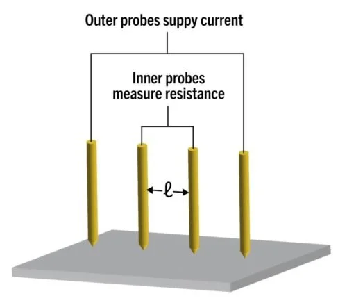
The purpose of this board was to provide a way to measure the resistivity of silver nano-wires using the four point probe method
This method consists of two sets of two probes, the outer two probes provide current and the center two probes measure the resistance (shown below)
The nature of the signals being measured meant that the overall PCB design had to be resistant to electromagnetic interference (EMI)
The following techniques were used to ensure EMI was minimized:
Having an uninterrupted ground plane as an internal layer
Reducing the length of return paths by placing the signal layers close to the return layers
Having decoupling capacitors near vias to reduce radiation stemming from return paths
Reduce loop inductance by placing power and ground plane close together in the layer stack
Ensure all the traces are terminated to avoid resonant issues
Minimize trace length for critical signals
Isolate digital and analog signals from one another
Use input and output filters to reduce high-frequency noise to/from cables
The board was an overall success and survived the very noisy environment. Results measured using this board can be found in this paper.